MYC-JX8MMA7
High-Speed Data Acquisition and HD Display with ARM+FPGA System-On-Module
Up to 1.8GHz NXP i.MX 8M Mini Quad ARM Cortex-A53 and 400MHz Cortex-M4 Cores
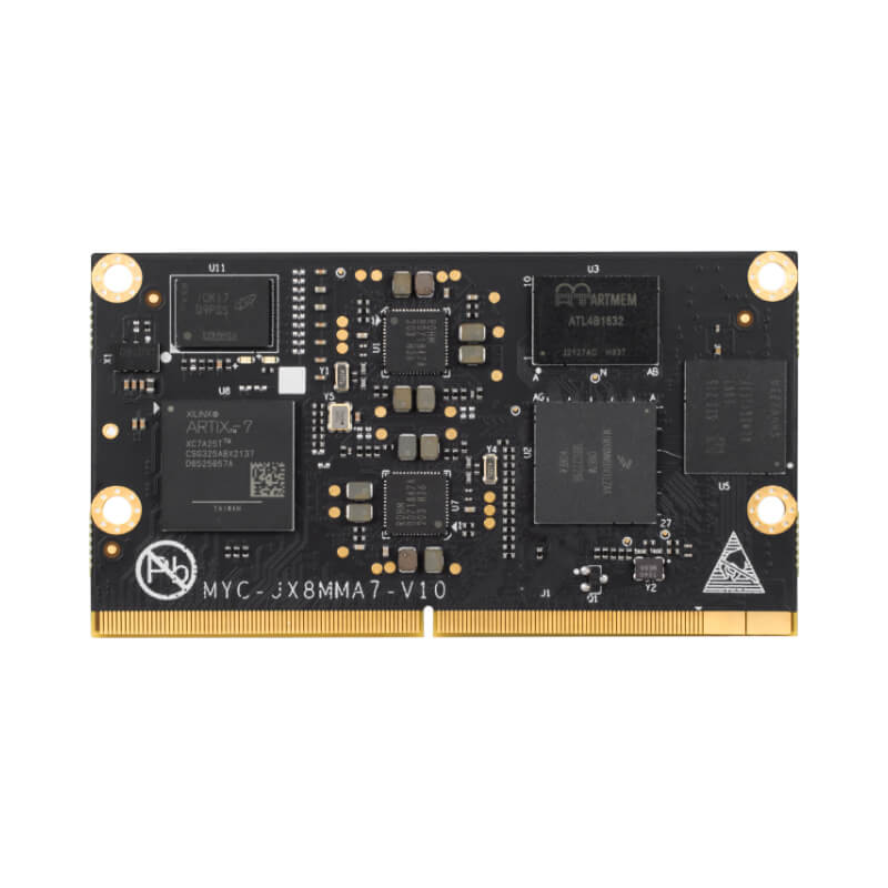
AMD/Xilinx XC7A25T Artix-7 FPGA
ARM: 2GB LPDDR4, 8GB eMMC and 32MB QSPI Flash
FPGA: 256MB DDR3 and 32MB QSPI Flash
Power Management IC
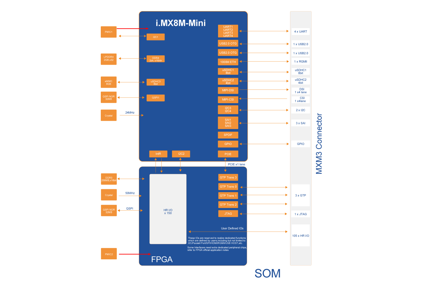
0.5mm pitch 314-pin MXM 3.0 Gold-finger-edge-card Connector
CE Certificated, Long-term Availability
Supports Running Linux OS
MYD-JX8MMA7 Development Board
NXP Approved Gold Partner
AMD Approved Adaptive Computing Partner


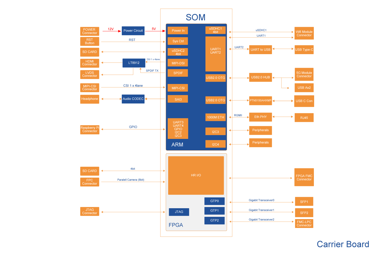
The Dual Architecture Features Both High-Speed Acquisition and High-Definition Display
MYC-JX8MMA7 SOM and development board are based on ARM+FPGA architecture, FPGA end is used to realize high-speed data acquisition and processing, ARM end is used to realize data processing, control, communication and display.
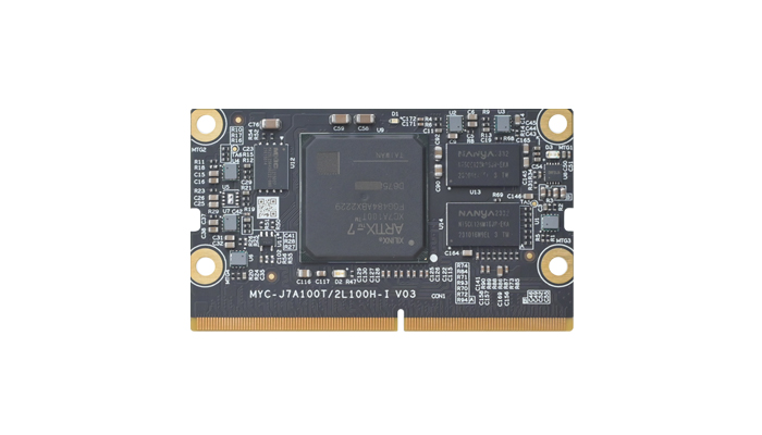
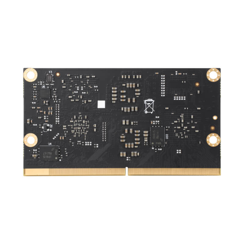
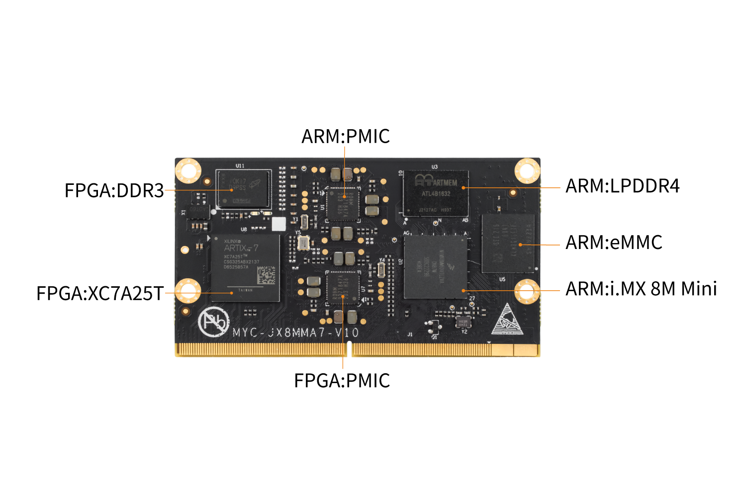
SOM - MYC-JX8MMA7
Measuring 82mm by 45mm, the MYC-JX8MMA7 SOM adopts the processing architecture of ARM+FPGA embedded system. It is a compact System-On-Module (SOM) based on 1.8GHz NXP i.MX 8M Mini quad-core ARM Cortex-A53 plus 400MHz Cortex-M4 processor and an integrated Xilinx XC7A25T Artix-7 FPGA. The SOM takes full advantages of the ARM MPU to provide powerful multimedia capability for data processing, control, communication and display, as well as enough FPGA resources for high-speed data acquisition, processing and AD module expansion.
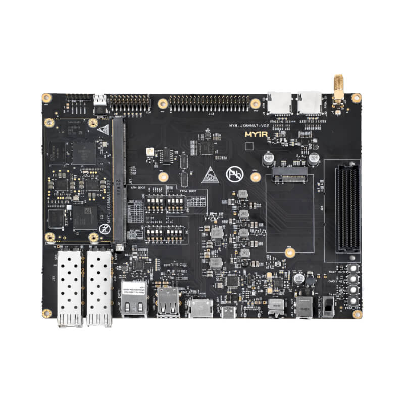
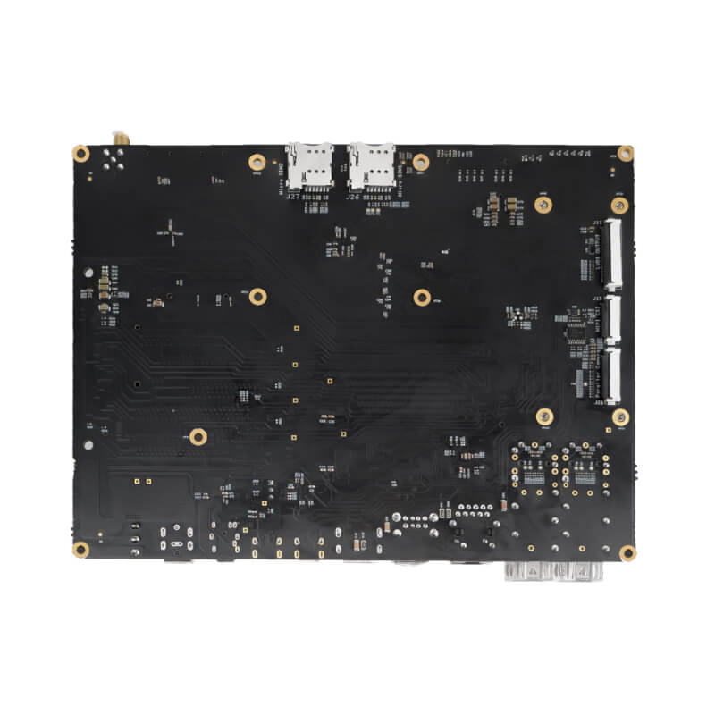
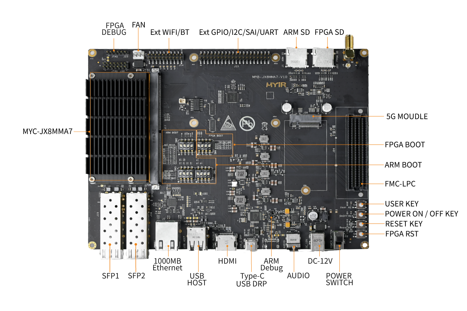
Development Board - MYD-JX8MMA7
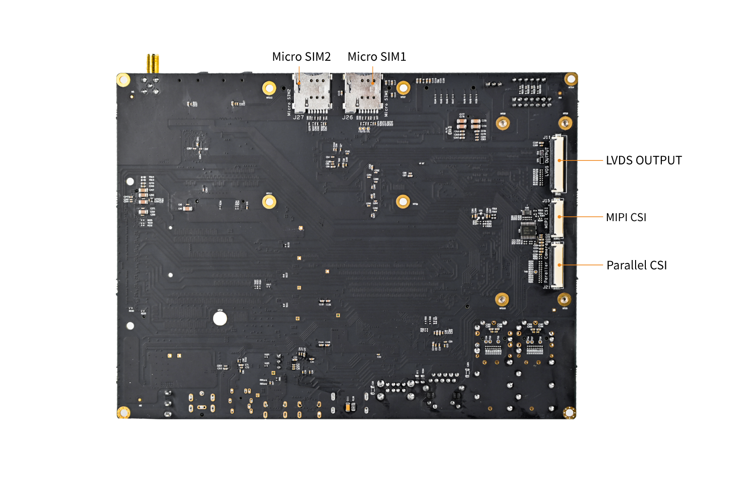
The MYD-JX8MMA7 development board provides a complete evaluation platform for the SOM. A plenty of peripherals interfaces are carried out to the base board like two USB Host and one OTG, one Gigabit Ethernet, two SFP network interfaces, WiFi/Bluetooth module interface, USB 2.0 based M.2 Key B 5G Module interface, LVDS and HDMI display interfaces, MIPI and Parallel CSI interfaces, Audio, one 2x 20-pin UART/I2C/SPI/GPIO extension header which is compatible with Raspberry Pi interface, etc.
Rich Development Resources
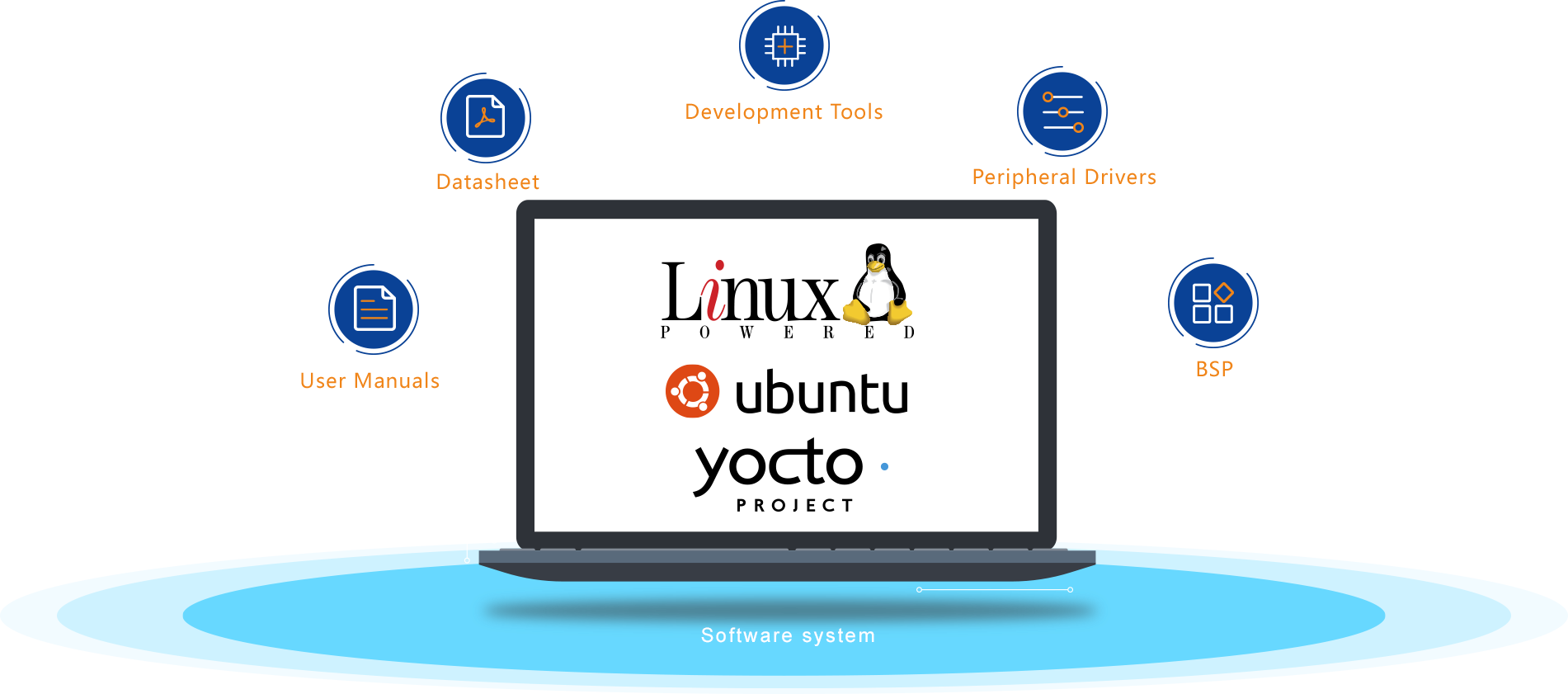
The software information for the MYC-JX8MMA7 SOM and development board includes, but is not limited to, U-boot, Linux, all peripheral driver source code, and QT5-based MEasy HMI V2.0 system-related development tools. The documentation comprises product manuals, hardware user manuals, hardware design guides, baseboard PDF schematic diagrams, as well as Linux software evaluation and development guides
Widely Used in Entry-level Embedded Systems
The MYC-JX8MMA7 SOM and development board are based on the ARM+FPGA processing architecture, with ARM processing performance as the main and FPGA as the auxiliary system. It is suitable for application scenarios with high requirements for data acquisition, multimedia and display, such as high-end medical equipment, industrial data acquisition systems, industrial control, radar, industrial gateways, robots, etc.

Industrial Gateway

Radar

Robot

High-end Medical Equipment

Industrial Control

Industrial Data Acquisition System
Download
| File Name | Type | Size | Download Links |
|---|---|---|---|
| MYC-JX8MMA7 Overview | 1.57 MB |

|
|
| MYD-JX8MMA7 Overview | 1.94 MB |
|
|
| CE Certification for MYC-JX8MMA7 SOM | 319.91 KB |
|
|
| 3D STEP File for MYC-JX8MMA7 SOM.rar | rar | 2.32 MB |
|
| MYD-JX8MMA7 Quick Start Guide | 2.34 MB |
|
Ordering
The sample price applies only to the first 2 pieces per customer. For any quantity beyond 2 pieces, the sample price no longer applies. Please contact us for pricing.
| SOMs | CPU | RAM | Flash | Working Temp. | Sample Price | Ordering |
|---|---|---|---|---|---|---|
| MYC-JX8MMA7-8E2D-32Q256D-180-C | ARM:MIMX8MM6DVTLZAA FPGA: XC7A25T-2CSG325C | ARM LPDDR4:2GB FPGA DDR3: 256MB | ARM eMMC :8GB FPGA QSPI Flash:32MB | 0~70℃ | USD125 |  |
| MYC-JX8MMA7-8E2D-32Q256D-160-I | ARM:MIMX8MM6DVTLZAA FPGA: XC7A25T-2CSG325C | ARM LPDDR4:2GB FPGA DDR3: 256M | ARM eMMC :8GB FPGA QSPI Flash:32MB | -40~85℃ | USD135 | |
| Development Boards | Packing List | With WiFi | Working Temp. | Sample Price | Ordering | |
| MYD-JX8MMA7-8E2D-32Q256D-180-C | * One MYD-JX8MMA7 board * One 12V/2A Power adapter * One USB TYPE-A to C cable * One DC Power jack adapter * One Quick Start Guide | No | 0~70℃ | USD199 | | |
| MYD-JX8MMA7-8E2D-32Q256D-160-I | No | -40~85℃ | USD209 | | ||
| Add-on Options | Description | Sample Price | Ordering | |||
| MY-LVDS070C | MY-LVDS070C 7-inch LCD Module with capacitive touch screen | USD79 | | |||
| MY-CAM003M | MY-CAM003M MIPI Camera Module | USD25 | | |||
| MY-CAM011B | MY-CAM011B BUS Camera Module | USD25 | | |||
| MY-WIREDCOM | MY-WIREDCOM RPI Module for extension of RS232/RS485/CAN | USD18 | | |||
| MY-WF005S | MY-WF005S WiFi/Bluetooth Module | USD18 | | |||
Similar Products