MYC-J7A100T
Compact System-On-Module (SOM) based on the Powerful AMD/Xilinx XC7A100T FPGA (XC7A100T-2FGG484I)
AMD/Xilinx XC7A100T Artix-7 FPGA (XC7A100T-2FGG484I)
512MB DDR3, 32MB QSPI FLASH, 32KB EEPROM
0.5mm Pitch 260-pin MXM Gold-finger-edge-card Connector
CE Certificated, Long-term Availability
Supports Development by Xilinx's Vivado Design Suite
MYD-J7A100T Development Board
AMD Approved Adaptive Computing Partner


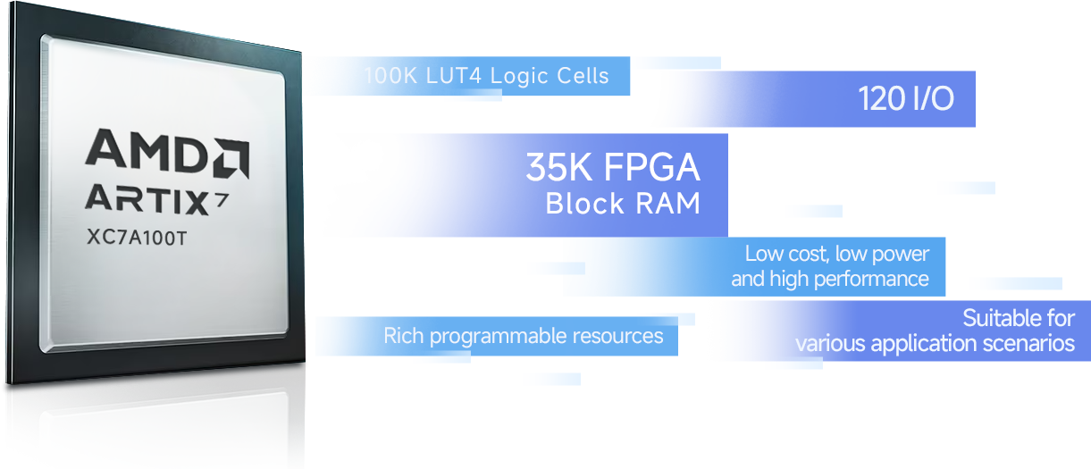
Equipped with abundant programmable resources, the XC7A100T-2FGG484I is a low-power, high-performance FPGA.
The XC7A100T-2FGG484I is an FPGA chip from the Artix-7 series, known for its cost-effectiveness, low power consumption, and high performance. It offers abundant programmable resources, including 100K logic cells, 35K FPGA storage units, and 120 I/O pins, making it suitable for a wide range of applications.
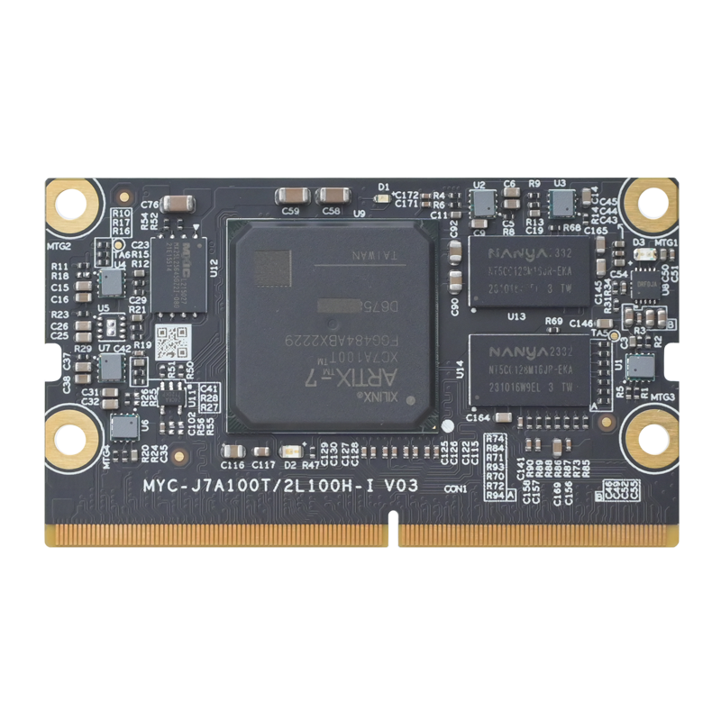
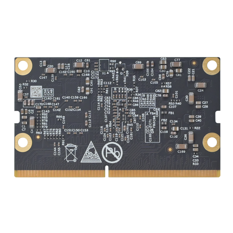
SOM - MYC-J7A100T
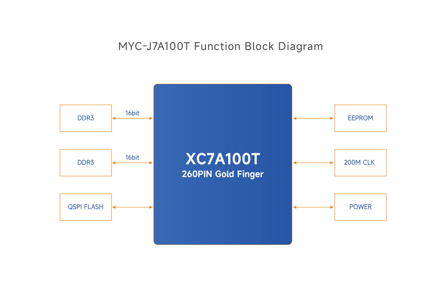
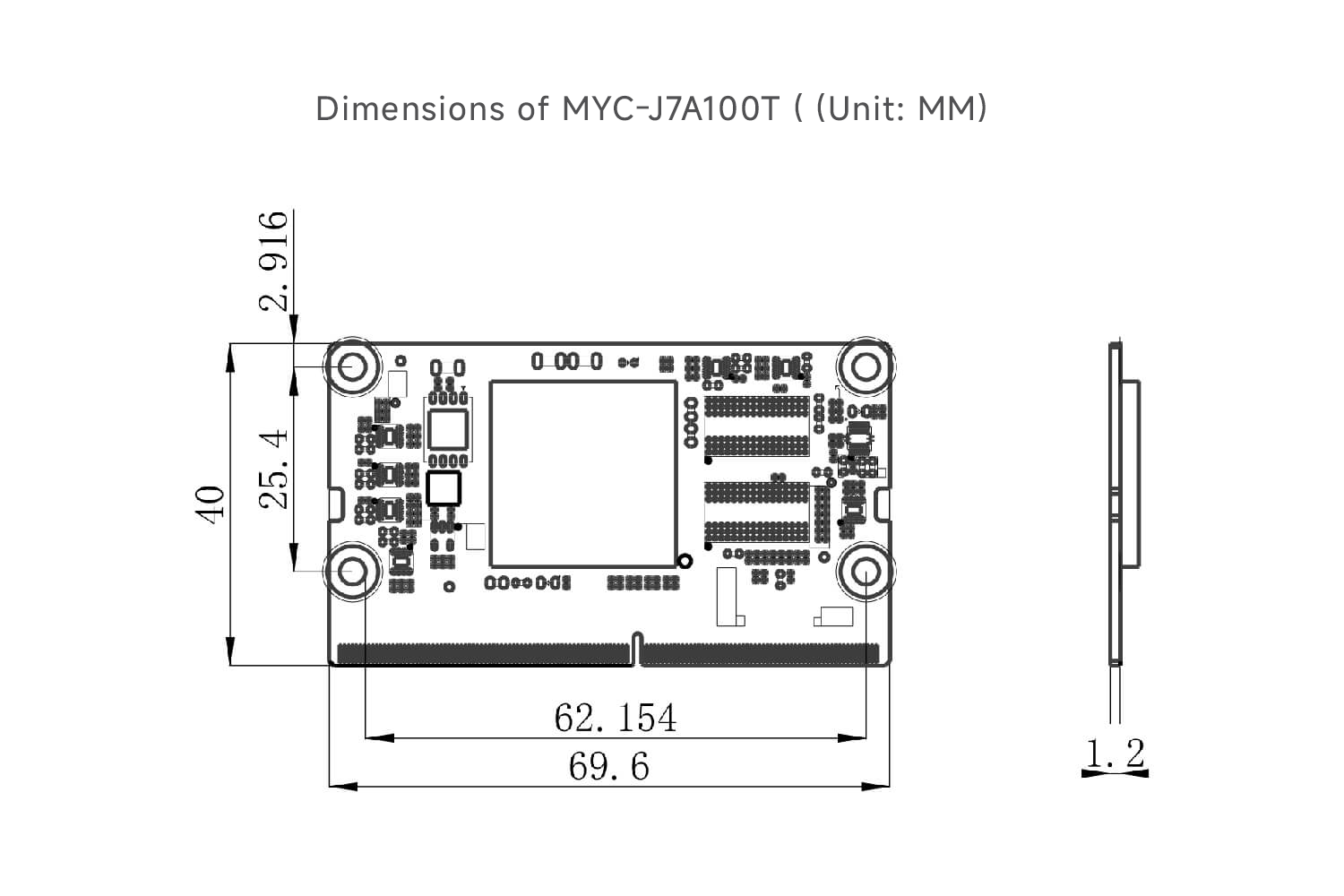
Measuring only 69.6mm by 40mm, the MYC-J7A100T is a compact System-On-Module (SOM) based on the powerful AMD/Xilinx XC7A100T FPGA (XC7A100T-2FGG484I), which belongs to the AMD Artix-7 family. Additionally, it features onboard 512MB DDR3, 32MB QSPI FLASH, and 32KB EEPROM. A variety of IO signals are available through the 0.5 mm pitch 260-pin MXM gold-finger-edge-card connector, facilitating easy connection with MYIR’s standard base board of the MYD-J7A100T development board or customized base boards from users. Furthermore, the MYC-J7A100T SOM provides a total of 178 FPGA IOs, 4 pairs of GTP high-speed transceiver interfaces, and one JTAG interface. Among the 178 FPGA IOs, 80 operates at 3.3V level, while the remaining 98 are user-configurable with various levels (1.2/1.35/1.5/1.8/2.5/3.3V).
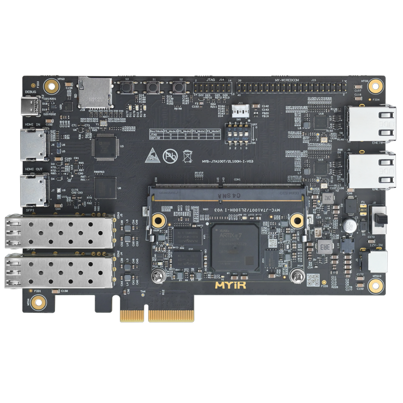
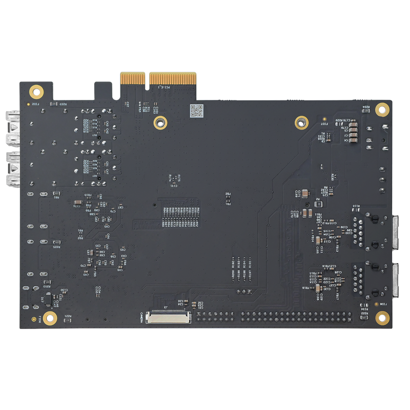
Development Board - MYD-J7A100T
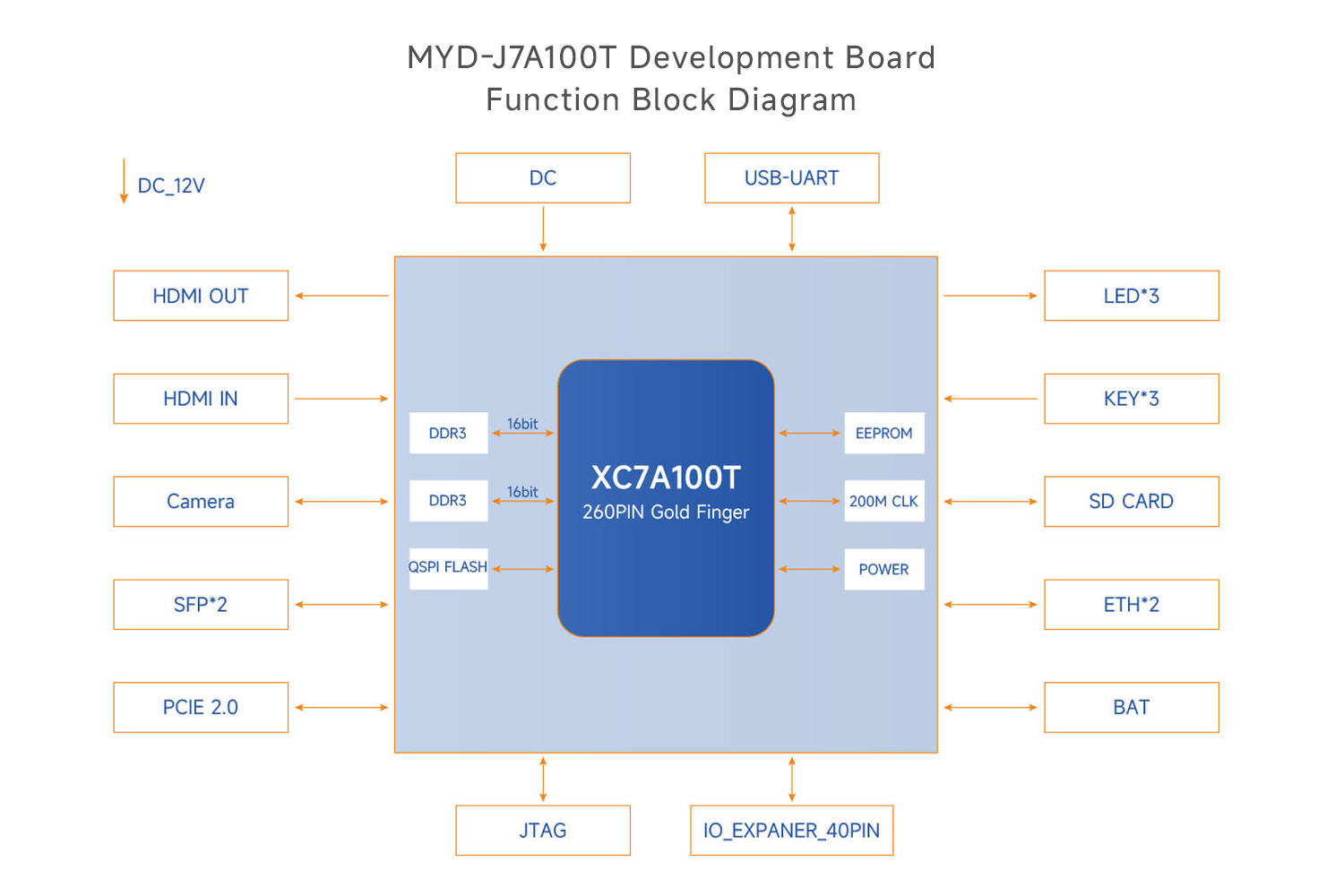
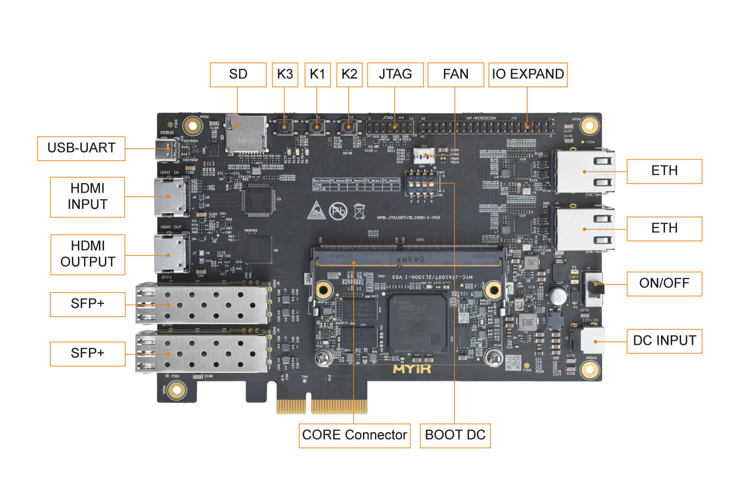
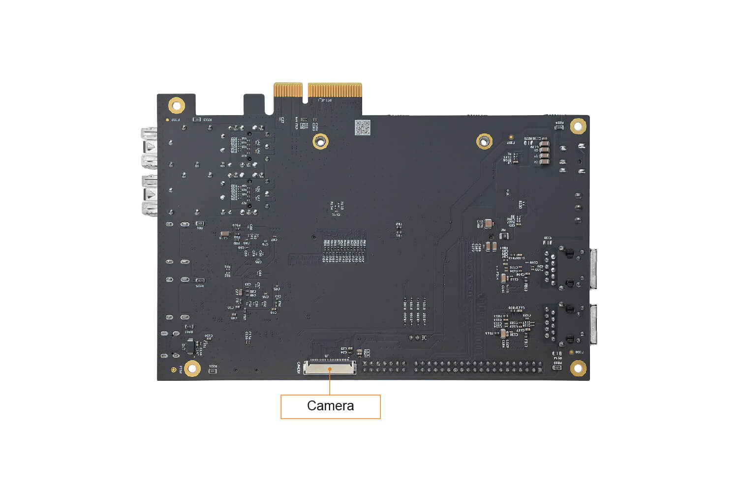
The MYD-J7A100T Development Board comprises the MYC-J7A100T SOM and a specially designed base board, which provides a fully equipped platform for evaluating and developing solutions based on AMD/Xilinx Artix-7 FPGAs. The MYD-J7A100T incorporates the XC7A100T (XC7A100T-2FGG484I) device from the Artix-7 series and extends a rich set of peripherals and interfaces on the base board through connectors and headers. These include two Gigabit Ethernet ports, two SFP+ interfaces, a PCIe 2.0 interface, HDMI input and output interfaces, a DVP camera interface, a Micro SD slot, a USB-UART interface, a FAN interface, and a 2.5mm pitch 2x 20-pin IO expansion interface.
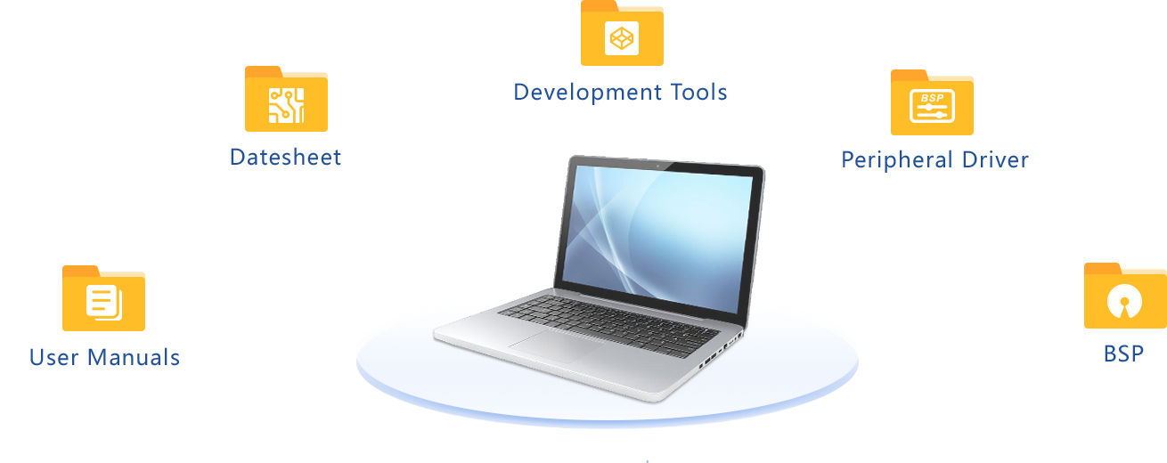
Rich Development Resources
The MYC-J7A100T SOM and development board come with a user manual, PDF schematic, development tools, and other related information. It offer a stable design reference and an optimal software development environment for developers.
Widely Used in Entry-level Embedded Systems
XC7A100T-2FGG484I has excellent performance and programmability, equipped with a wealth of peripheral interfaces, low power consumption, high performance, suitable for industrial control, automation, communication, computer and other fields.

Communication

Industrial Control

Automation

Computer

Medical

Machine Vision
Download
| File Name | Type | Size | Download Links |
|---|---|---|---|
| MYC-J7A100T Overview | 1.07 MB |

|
|
| MYD-J7A100T Overview | 1.41 MB |
|
|
| CE Certification for MYC-J7A100T SOM | 2.54 MB |
|
|
| 3D STEP File for MYC-J7A100T SOM.rar | rar | 1.3 MB |
|
| MYD-J7A100T Quick Start Guide | 114.11 MB |
|
Ordering
The sample price applies only to the first 2 pieces per customer. For any quantity beyond 2 pieces, the sample price no longer applies. Please contact us for pricing.
| SOMs | CPU | RAM | Flash | Working Temp. | Sample Price | Ordering |
|---|---|---|---|---|---|---|
| MYC-J7A100T-32Q512D-I | XC7A100T-2FGG484I | 512MB DDR3 | 32MB QSPI FLASH | -40~85℃ | USD125 |  |
| Development Boards | Packing List | With WiFi | Working Temp. | Sample Price | Ordering | |
| MYD-J7A100T-32Q512D-I | *One MYD-J7A100T board (including MYC-J7A100T SOM) * One USB Type A to Type cable * One 12V/2A Power adapter * One Quick Start Guide | No | -40~85℃ | USD169 | | |
| Add-on Options | Description | Sample Price | Ordering | |||
| MY-WIREDCOM | MY-WIREDCOM RPI Module for extension of RS232/RS485 | USD18 | | |||
| MY-CAM011B | MY-CAM011B Camera Module | USD25 | | |||
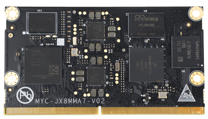
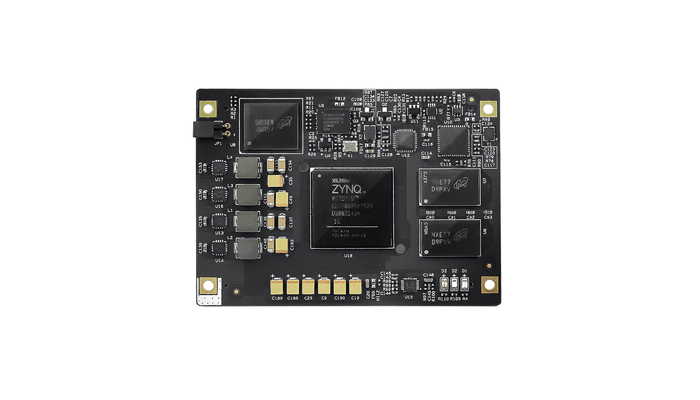
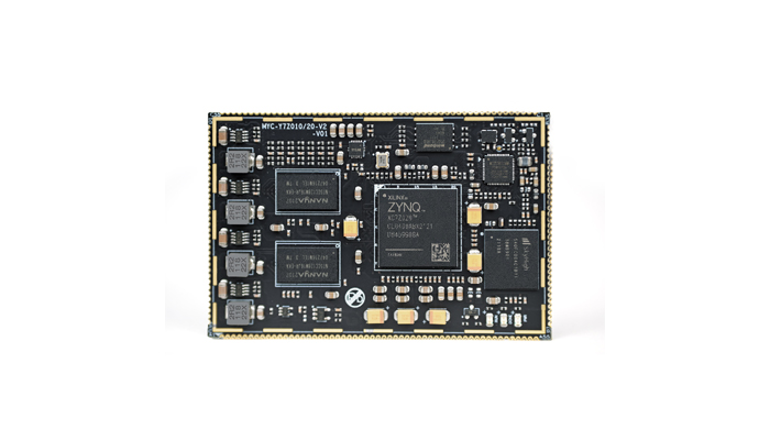
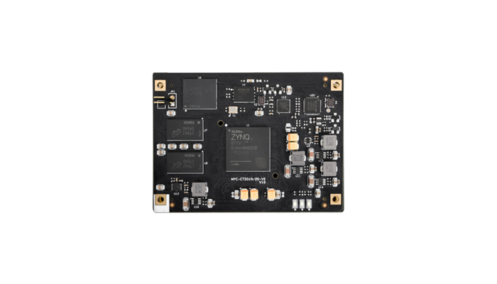
Similar Products